- Samsung reportedly uses MUF tech for its HBM chip production.
- However, Samsung has denied using MUF tech, calling it a rumor.
Samsung reportedly uses MUF tech for its HBM chip production. However, Samsung has denied using MUF tech, calling it a rumor.
Samsung is said to use chip-making tech its rival favoured
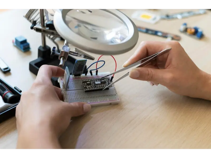
The growing demand for high bandwidth memory (HBM) chips has surged due to the ongoing popularity of generative AI. In this context, Samsung Electronics plans to utilize a chip-making technology favored by its rival, SK Hynix.
According to analysts and industry experts, one reason for Samsung’s lagging behind is its persistence in using a chip-making technology called non-conductive film (NCF), which has caused some production problems. In contrast, Hynix has addressed NCF’s weaknesses by employing the mass reflow molded underfill (MR-MUF) method.
“Samsung had to do something to ramp up its HBM production yields… adopting the MUF technique is a bit of a swallow-your-pride move for Samsung because it ended up following the technique first used by SK Hynix,” one source said.
Also read: OpenAI’s Altman to meet chipmakers Samsung
Samsung denied the rumour that it will use MUF
Samsung is reportedly achieving about 10-20% yield rates for its HBM3 production, lagging behind Hynix, whose chip production rate is secured at about 60-70%, according to analysts. However, Samsung has denied the estimated data and claimed it has secured a “stable yield rate.”
As things stand, Samsung’s NCF tech is the “best solution” for HBM products to be used in the new HBM3E chips. “We are carrying out our HBM3E product business as planned,” Samsung said in response to Reuters’ questions on the article. However, after the article was published, Samsung stated, “Rumors that Samsung will apply MR-MUF to its HBM production are not true.”