
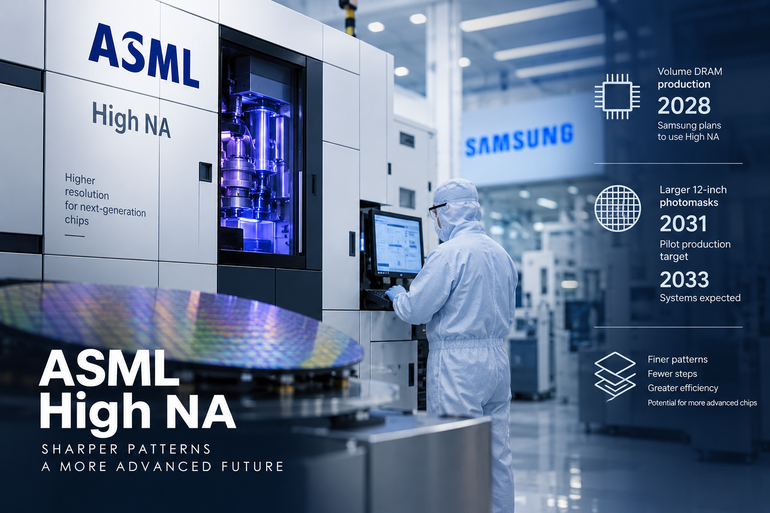
- Samsung plans to bring High NA into volume DRAM production from 2028 as ASML gains more customer commitments
- Larger 12-inch photomasks remain on a separate timetable, with early High NA systems continuing to use the current mask format
The fact
ASML's High NA lithography machines are gaining commitments from leading chipmakers, Reuters reported on 14 September. The systems offer finer resolution than existing EUV equipment and cost about $400 million each, roughly twice the price of current EUV tools.
Samsung and ASML said on 8 September that they would expand their High NA work, with Samsung planning to introduce the technology into volume DRAM production from 2028. The companies are also developing a larger 12-inch photomask format intended to support bigger chip layouts and reduce the need to stitch separately printed areas together.
Those developments are on different schedules. Early High NA production systems will continue using the existing six-inch mask format. Reuters reported a 2031 target for pilot production with the larger masks, followed by systems supporting them in 2033.
The assessment
Samsung’s 2028 DRAM rollout will be one of the first chances to see whether High NA can justify its much higher price in volume manufacturing. A roughly $400 million lithography tool only makes sense if it saves enough time or complexity elsewhere in production. If Samsung can remove patterning steps without giving up too much throughput or yield, the higher equipment cost may be easier to absorb. How well that works will depend on the particular chip and manufacturing process.
The larger photomask follows a separate timetable. Samsung can start using High NA with the current six-inch mask format, so its 2028 DRAM plans do not depend on the 12-inch version being ready. Chipmakers can therefore introduce the technology in stages rather than wait for the entire roadmap to arrive.
For BTW readers, customer commitments show that High NA is moving closer to regular production. The stronger evidence will come from the fab itself: whether Samsung can reduce process steps, keep wafers moving through the line and maintain enough yield to make the investment worthwhile.
What to watch
Samsung's move towards volume DRAM production in 2028 is the next major test. Watch for evidence on process-step reductions, throughput and yield once High NA enters production. Progress on 12-inch masks should be tracked separately against the reported 2031 pilot and 2033 system targets.
Member Briefing
Deeper Profile Context
Sign in with the right membership level to unlock the full briefing and source notes.
Only for Strategic Circle
Strategic Circle
Open to all readers. Unlock profile briefings after joining and signing in.
Join Strategic CircleOnly for Leadership Alliance
Leadership Alliance
For qualified IP-asset owners and management; sign in to unlock alliance briefings.
Join Leadership Alliance