
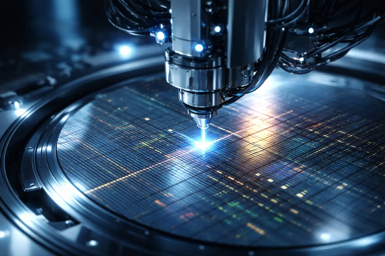
Microsoft-backed startup raises $40 million to develop advanced chipmaking equipment, signaling strategic interest in semiconductor infrastructure. This move underscores the growing importance of manufacturing capabilities and tool innovation for meeting AI, cloud computing, and data center expansion demands.
- Lace Lithography—not an unnamed Microsoft-controlled supplier—raised a $40 million Series A led by Atomico. Microsoft's connection is an investment by venture arm M12; no cited source establishes a Microsoft procurement commitment, customer role or control over the technology.
- Lace replaces light with a neutral helium-atom beam for semiconductor patterning. It has prototype systems and research validation, while the stated milestone is a test tool in a pilot fab around 2029. Resolution claims are potential outcomes, not production yield or throughput results.
The financing has a name, stage and investor boundary
A Reuters report republished by Sahm Capital identifies the company as Norway-headquartered Lace Lithography and the financing as a $40 million Series A. Atomico led the round; entities named in that report include Microsoft's M12, Linse Capital, Spain's Society for Technological Transformation and Nysnø. Lace declined to disclose its valuation. Calling the company merely “Microsoft-backed” hides both the lead investor and the limited meaning of a venture investment.
Lace is changing the exposure source, not selling a generic efficiency tool
Conventional lithography projects a pattern onto a resist-coated wafer. Lace's company description calls its approach BEUV, or Beyond-EUV, and uses atoms instead of photons. Reuters says its engineers use a neutral helium-atom beam about 0.1 nanometres wide. Chief executive and co-founder Bodil Holst says the method could print features at ultimately atomic resolution; Imec lithography director John Petersen told Reuters it could enable features an order of magnitude smaller. Those are expert and company assessments of potential, not measured production specifications.
The underlying research is real, but the maturity is bounded
The European Commission's FabouLACE project record describes metastable-atom, mask-based lithography at proof-of-concept stage, with a prototype and TRL 6 validation goal involving Imec and end users. A University of Bergen doctoral record documents the design, construction and characterisation of a metastable-helium lithography instrument. The published European patent application names Lace Lithography as applicant for particle-beam shaping technology. Grants, a dissertation and a patent establish a research and intellectual-property base; they do not establish a production-qualified scanner.
EUV is an industrial benchmark, not just a wavelength comparison
ASML's EUV product record says its established systems use 13.5-nanometre light, with NXE tools used in high-volume manufacturing and High-NA EXE systems designed for advanced production. Comparing that light wavelength with the reported width of Lace's atom beam does not directly compare printable critical dimension, overlay, defects or throughput. An exposure source becomes a manufacturing tool only when source stability, masks, resist response, wafer stages, vacuum, contamination control, metrology, inspection and process control work together.
The next disclosed milestone is a pilot tool, not mass production
Reuters says Lace has built prototype systems and aims to place a test tool in a pilot fab around 2029. Tom's Hardware's independent assessment highlights the absence of an existing process ecosystem and the long gap between prototype and volume production. The funding can pay for engineering, hiring and integration, but it does not prove a 300-millimetre wafer workflow, acceptable wafers per hour, overlay and critical-dimension uniformity, defect density, resist compatibility, uptime, maintainability, yield or cost of ownership.
M12 backing is not a supply agreement
M12's portfolio page confirms Lace as an investment. None of the reviewed sources says Microsoft will buy the equipment, reserve output, transfer process technology or direct Lace's roadmap. The financing therefore demonstrates investor appetite for a long-horizon semiconductor equipment bet; it does not demonstrate that Microsoft has secured chip supply or that Lace will displace ASML.
What would turn the physics into a manufacturing case
The decisive evidence will arrive in stages: repeatable patterns on relevant resists and wafers; independent resolution, line-edge roughness, overlay and defect measurements; stable source power and mask life; integration with metrology and process-control systems; a named pilot fab and customer qualification; and throughput, uptime, yield and cost data. Patent progress, prototype milestones and hiring matter, but the 2029 test-tool target and any later production date should remain explicitly labelled as plans until those results are published.
Why the funding matters
Lithography is a tightly coupled manufacturing control surface, and an alternative exposure mechanism could matter if it extends scaling at workable productivity and cost. Lace now has more capital and a credible research lineage to attempt that transition. The round does not by itself make semiconductor supply chains more resilient, guarantee cheaper or more powerful chips, create stable investor returns or settle export-control dependencies. The investable event is funding for an ambitious prototype-to-pilot programme, with technical and commercial risk still concentrated ahead.
Member Briefing
Deeper Profile Context
Sign in with the right membership level to unlock the full briefing and source notes.
Only for Strategic Circle
Strategic Circle
Open to all readers. Unlock profile briefings after joining and signing in.
Join Strategic CircleOnly for Leadership Alliance
Leadership Alliance
For qualified IP-asset owners and management; sign in to unlock alliance briefings.
Join Leadership AllianceSnapshot
Category
InstitutionRegion
ASIA PacificSignal Focus
MarketContent Type
ProfilePrimary Domain
TechnologyTopic
MarketImpact
HighConfidence
Limited confidence (82%)Confidence score guide
Several public sources