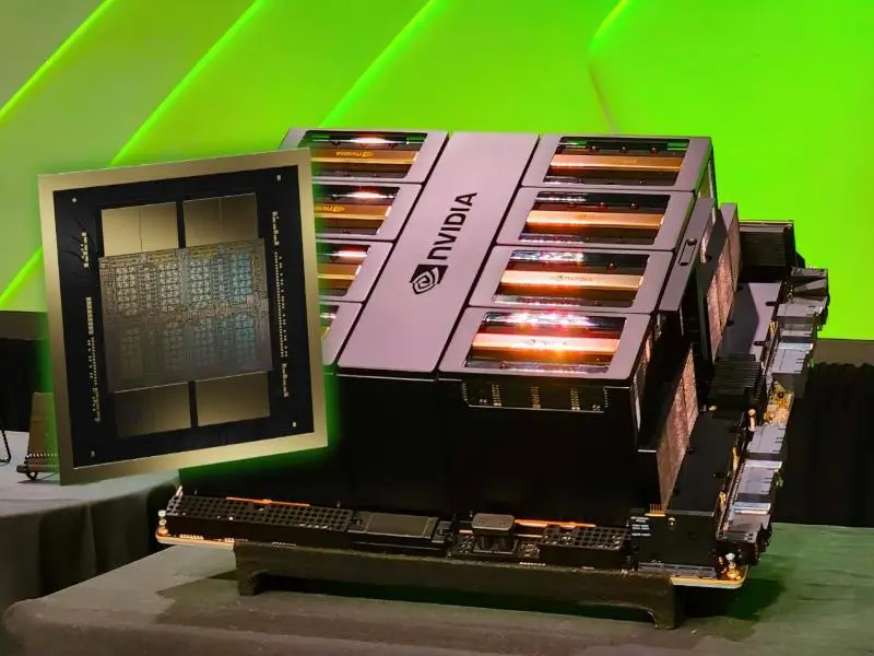
- A version of Samsung Electronics’ fifth-generation high bandwidth memory (HBM) chips, or HBM3E, has passed Nvidia’s tests for use in its artificial intelligence processors, three sources briefed on the results said.
- This development marks a significant milestone in the collaboration between the two tech giants and signals a step forward in the advancement of AI technology.
OUR TAKE
Nvidia is a pioneering company in the field of graphics processing units (GPUs) and AI processors, dedicated to advancing computing technologies for a wide range of applications. Samsung Electronics is a world-renowned manufacturer of consumer electronics and semiconductors, known for its innovative and cutting-edge products that drive industry progress. Samsung’s HBM3E chips in Nvidia’s AI processors promise faster speeds, better efficiency, and the ability to manage larger, more intricate AI models, propelling AI innovation forward.
–Rebecca Xu, BTW reporter
What happened
According to three sources briefed on the matter, a variant of Samsung Electronics’ next-generation high bandwidth memory (HBM) chips, known as HBM3E, has successfully cleared Nvidia’s assessments for integration into its artificial intelligence processors.
Though Samsung and Nvidia have not yet formalised a supply agreement for the tested 8-layer HBM3E chips, insiders anticipate that the deal will be sealed shortly, with deliveries projected to commence in the fourth quarter of 2024.
HBM, a DRAM (dynamic random-access memory) standard introduced in 2013, stacks chips vertically to save space and reduce power usage. It is integral to GPUs for AI, aiding in processing large data volumes from intricate applications. HBM3E chips are likely to become the mainstream HBM product in the market this year with shipments concentrated in the second half, according to research firm TrendForce.
Also read: Samsung forecasts AI-driven chip demand surge
Also read: Nvidia’s AI chip delay is a supply chain test for AI technology
Why it’s important
The adoption of Samsung’s 8-layer HBM3E chips by Nvidia is set to significantly impact the future of AI technology, particularly in enhancing performance and efficiency.
Firstly, the HBM3E chips offer a substantial increase in memory bandwidth, which is crucial for AI processors handling complex workloads. The chips provide a data rate of 9.6Gb/s, which is an improvement over the 6.4Gb/s offered by HBM3, leading to over 1200GB/s of memory bandwidth compared to 819GB/s of the previous generation . This leap in bandwidth allows for the processing of larger and more sophisticated AI models, thereby enhancing the performance of AI applications.
Secondly, the HBM3E chips are designed with advanced technologies such as high-k metal gates (HKMG) that reduce electrical current leakage, optimising internal circuitry and improving power efficiency by 12% compared to the previous generation . This increase in efficiency is vital for AI processors that require high memory bandwidth at lower power consumption, ensuring that they can perform at optimal temperature ranges without compromising on performance.
Moreover, Samsung’s HBM3E chips are the world’s first and are 50% faster than current HBM3, delivering a total of 10TB/sec of combined bandwidth. This allows the new platform to run models 3.5x larger than the previous version, while improving performance with 3x faster memory bandwidth . The ability to connect multiple GPUs for exceptional performance and easily scalable server design further amplifies the potential for AI processors to tackle more extensive generative AI workloads.

