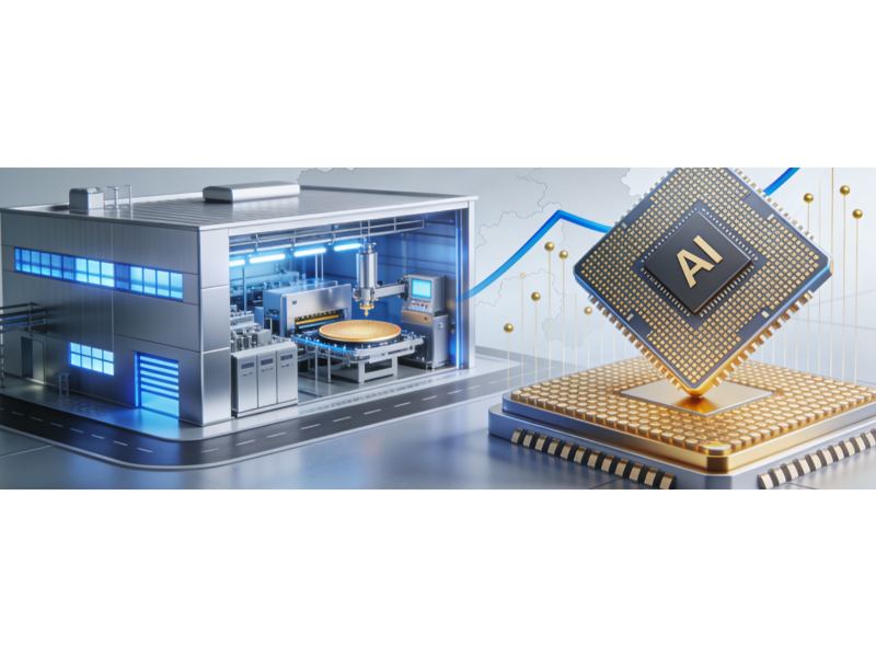
• South Korean memory maker SK Hynix announced a 19 trillion won (about $12.9 billion) investment to build a new advanced packaging facility aimed at boosting production of high-bandwidth memory (HBM) for AI systems.
• The new plant, set to begin construction in April 2026 in Cheongju, highlights intensified competition in semiconductor capacity but raises questions about risks of oversupply and timing.
What happened: new packaging investment
South Korea’s SK Hynix Inc. has unveiled plans to invest about 19 trillion won (approximately $12.9 billion) in a new advanced semiconductor packaging facility in Cheongju, as part of its strategy to meet burgeoning demand for memory chips used in artificial intelligence and high-performance computing.
The facility, known internally as P&T7, will focus on packaging and testing high-bandwidth memory (HBM) products — specialised memory used to handle large volumes of data in AI accelerators and data-intensive workloads. Construction is scheduled to begin in April 2026 with the company targeting completion by the end of 2027.
HBM is a form of dynamic random-access memory (DRAM) that stacks memory dies vertically, enabling faster data throughput and lower power consumption compared with traditional memory technologies. SK Hynix is currently one of the largest suppliers of HBM globally, holding a majority market share and serving top AI hardware clients including Nvidia.
The new packaging hub is intended to complement SK Hynix’s existing front-end wafer fabs — including the M15X fabrication facility also in Cheongju that has recently expanded next-generation DRAM capacity. Linking packaging closely with front-end production can reduce logistics costs, improve production yields and shorten the time it takes to deliver finished memory products to customers.
In its announcement, SK Hynix said the investment aligns with broader national industrial goals and supply chain efficiencies, as well as the structural shift in the semiconductor market towards more advanced memory solutions required by AI and high-performance computing systems.
SK Hynix’s share price dipped slightly on the Korea Exchange following the announcement, as investors weighed near-term financial impacts against long-term strategic positioning in the AI memory segment.
Also Read: SK Hynix ramps up chip packaging capacity in South Korea
Also Read: South Korean L&F slashes value of Tesla battery material supply deal to $7,386
Why it’s important
The packaging plant investment reflects a wider global trend where memory and semiconductor companies are seeking to vertically integrate back-end operations — processes such as stacking, testing and final assembly — alongside traditional front-end wafer manufacturing. For complex products like HBM, efficient back-end packaging is a critical differentiator in performance and profitability.
HBM demand has surged rapidly as AI workloads grow more complex and data-intensive, driving memory makers to expand capacity. Market research suggests that the HBM segment could grow strongly through the end of the decade. SK Hynix’s near-dominant position in the HBM market underscores why the company is prioritising a large packaging investment over this period.
However, there are risks. A large capital expenditure on packaging amid what industry participants describe as a potentially cyclical memory market means SK Hynix — like rivals such as Samsung Electronics and Micron Technology — must balance capacity expansion with the risk of oversupply. Memory markets have historically experienced boom-bust cycles when capacity expands sharply in response to rising demand, only for demand growth to slow shortly thereafter.
Timing is also a variable. The new facility will not be operational until late 2027, by which point the competitive landscape and AI memory requirements could shift further. Integration with front-end fabs and ensuring consistent quality and yield of HBM products will be essential for SK Hynix to justify its large investment against both supply chain bottlenecks and competitor plans.
There are also geopolitical and supply chain considerations. Memory chips and advanced packaging are now strategic technologies tied to broader national industrial policies, particularly in East Asia. South Korea’s support for SK Hynix’s investment signals continued emphasis on semiconductor leadership, but it also draws scrutiny over whether such capacity expansions foster sustainable competition or contribute to future market imbalances.

